Microcontroller projects
RISC-V assembler on bare metal Pi Pico 2 (RP2350)
last updated: 2025-10-29
Work in progress
Intro
The latest political signals from China (pact with dictators Putin and Kim Jong-un) lead me to believe that it is time to boycott as far as possible Chinese microcontrollers. America is no longer the friend to Europe, with M. Trump as president. American Tech Giants get too greedy.
It is time to change. Linux as OS and RISC-V for our microcontroller. And as far as possible no more chinese or american products.
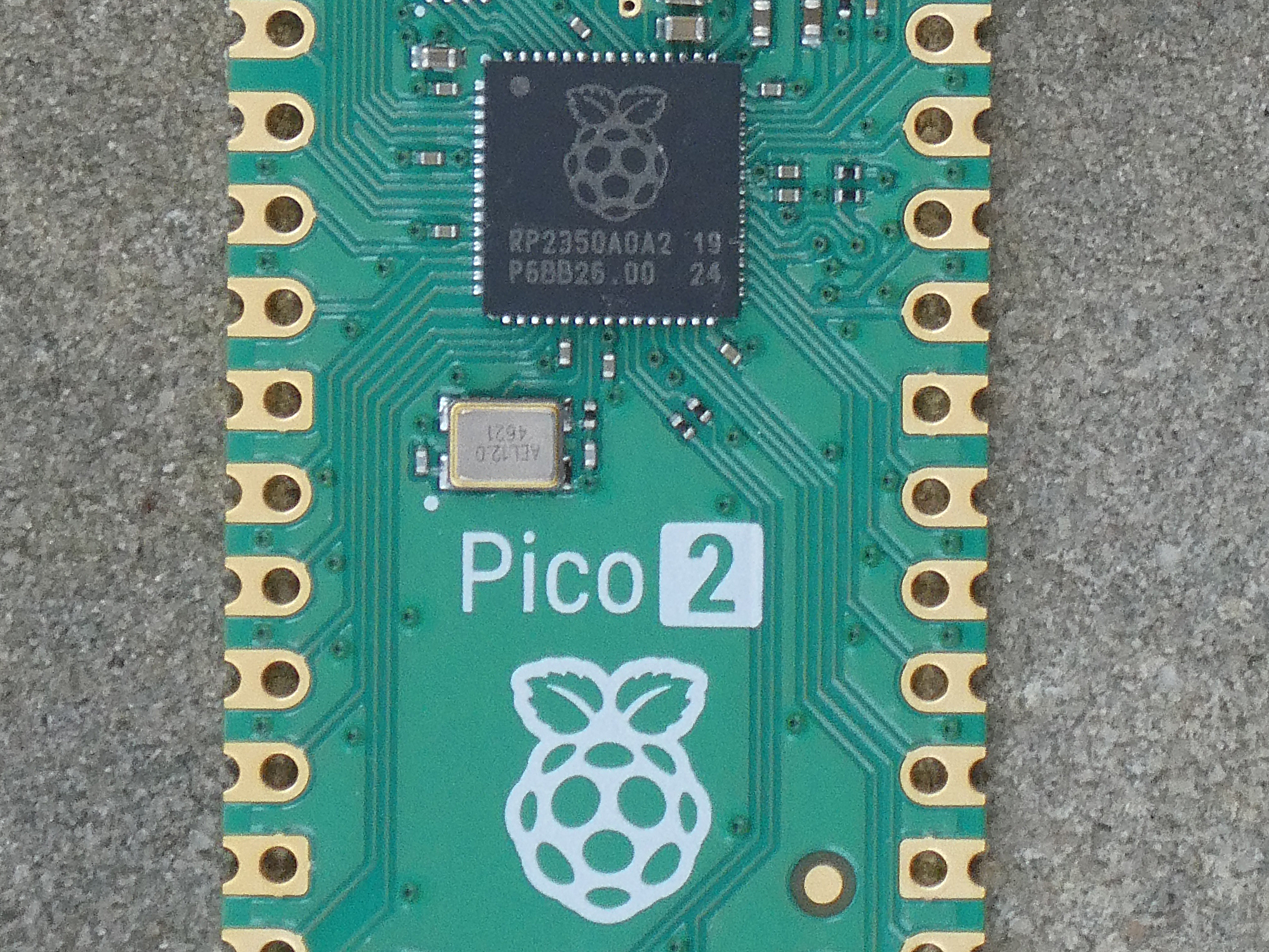
The new Raspberry Pi Pico 2 processor (RP2350) was designed in Europe and has beneath ARM cores 2 RISC-V (Hazard3, RV32IMAC+) cores. So let’s use them.
And here we will not use the SDK but get back to the real basics! Bare metal as its best and it must hurt (and we want to learn something and have fun ;)!
The code in assembler refers to a special chip. It is not portable like high level languages. So the data sheet of RP2350 is our friend and I will mention the interesting chapters in parentheses.
We use the RISC-V cores with RISC-V assembler! You can not use directly programs written for the RP2350, so even if you find assembler code for the RP2350 it is often code for the ARM cores.
I had problems to find documentation how to do this bare metal in the RP2350 and most of the suggestions of an AI is useless! That’s why I’m documenting this.
I combed the net and found only one valuable source for RISC-V bare metal. A blog called Wolfmans Howlings. And naturally the cool videos from Life with David on bare metal on the Pico with arm: Thanks wolfman and david, your code and infos worked and helped a lot to start.
Now let’s go to work.
Please look here: https://www.weigu.lu/microcontroller/pico_risc-v/index.html to create the udev rules and install openOCD to program the Pico 2 with a Debugprobe.
Installing the RISC-V toolchain
Everything here is done on a Linux machine (Kubuntu, resp. Debian). If you have no Linux machine, install some in a virtual box or use a Raspberry Pi 5 with Pi OS for this.
We need a 32 bit toolchain for the Hazard3 core on the Raspberry Pi Pico 2 (RP2350).
We will use the GNU toolchain.
One of the key components of that toolchain is the GNU Compiler Collection(GCC). We will refer to it as GCC in this document. It contains beneath the preprocessor and linker the GNU Assembler.
The ISA supported by Hazard3 is rv32imac ( The easiest way is to use a pre-built toolchain from the jenkins server of embecosm.com. We download it in our own directory and extract the file:
mkdir -p ~/pi_pico2/risc_v_gcc
cd ~/pi_pico2/risc_v_gcc
wget https://buildbot.embecosm.com/job/corev-gcc-ubuntu2204/83/artifact/ \
corev-openhw-gcc-ubuntu2204-20250302.tar.gz
tar -xzf corev-openhw-gcc-ubuntu2204-20250302.tar.gz
Open a new terminal and test the assembler with:
cd ~/pi_pico2/risc_v_gcc/corev-openhw-gcc-ubuntu2204-20250302/bin/ \
riscv32-corev-elf-gcc --version
Add the following line to your ~/.bashrc file:
export PATH="$PATH:/home/weigu/pi_pico2/risc_v_gcc/ \
corev-openhw-gcc-ubuntu2204-20250302/bin"
Let’s toggle an GPIO output (RISC-V)
Let’s try with our own minimal code. The code should allow to easily change the pin. And we want to do it as fast as possible :). Explanations will follow after the cool work is done, and naturally iterations to reach our goal:
 1
 2
 3
 4
 5
 6
 7
 8
 9
10
11
12
13
14
15
16
17
18
19
20
21
22
23
24
25
26
27
28
29
30
31
32
33
34
35
36
37
38
39
40
41
42
43
44
45
46
47
48
49
50
51
52
53
54
55
56
57
58
59
60
61
62
63
64
65
66
67
68
69
70
71
72
73
74
75
76
77
78
79
80
81
82
83
84
85
86
87
88
89
90
91
### Toggle an GPIO pin (minimal version)
### 01_toggle.S
### weigu.lu

        ### RP2350 Image Definition Block
        # This block is required for the RP2350 to recognize the binary as a valid
        # RISC-V executable. It must appear within the first 4 KB of the image.
        # RP2350 data sheet: 5.9.1. Blocks and block loops
        # 5.9.3. Image definition items, 5.9.3.4. ENTRY_POINT item
        .p2align 8       # Align to 8-byte boundary (required for RP2350 image header)
        .word 0xffffded3 # Header magic number (identifies the image)
        .word 0x11010142 # Item 0 flags: 0b0001 0001 0000 0001 0000 0100 0010
                         # IMAGE_TYPE_EXE, EXE_SECURITY_UNSPECIFIED,
                         # EXE_CPU_RISC,  EXE_CHIP_RP2350
        .word 0x00000344 # Item 1: Block size = 3,
                         # Block type = PICOBIN_BLOCK_ITEM_1BS_ENTRY_POINT
        .word _start     # Item 2: Inital PC (runtime) address (aka entry point)
        .word _stack_top # Item 3: Initial SP address (aka stack pointer)
        .word 0x000004ff # Item 4: Optional SP limit address (aka stack limit)
        .word 0x00000000 # Link: Single block loop has 0 items
        .word 0xab123579 # Footer magic number

         ### Global vars
        .equ PIN_OUT, 15                    # Pin to use
        .equ DELAY_NUMBER,    1000000       # 1000000 gives us ~ 2 Hz (12MHz clock)

        .section .text              # Marks the start of the code section in memory
        .global _start              # Makes the symbol '_start' visible to the linker

        ### Masks and Offsets
        .equ GPIO_MASK,       (1 << PIN_OUT)# Bitmask for GPIO (e.g. GPIO15 = bit 15)
        .equ GPIO_OFFSET,     PIN_OUT*8+4   # Offset for GPIO reg. (0=Status, +4=Ctrl)
        .equ PADS_OFFSET,     PIN_OUT*4+4   # Offset for PAD reg. (GPIO0 starts w. +4)
        .equ ATOMIC_XOR,      0x1000        # atomic offset bitmask XOR toggle on wr.
        .equ ATOMIC_SET,      0x2000        # atomic offset bitmask OR (set) on write
        .equ ATOMIC_CLR,      0x3000        # atomic offset bitmask AND on write
        .equ PAD_MASK_ISO_BIT,0x100         # Bit 8 = Pad Isolation control

        ### Memory-Mapped Register Definitions
        .equ IO_BANK0_BASE,   0x40028000    # IO Bank0 Base Address
        .equ GPIO_CTRL,       IO_BANK0_BASE + GPIO_OFFSET # GPIO_CTRL reg. (for Mux)
        .equ SIO_BASE,        0xD0000000    # SIO (Single-Cycle I/O) Base Address
        .equ GPIO_OUT_XOR,    SIO_BASE + 0x28 # GPIO output XOR register (atomic)
        .equ GPIO_DIR,        SIO_BASE + 0x30 # GPIO direction register
        .equ GPIO_DIR_SET,    SIO_BASE + 0x30 + ATOMIC_SET # GPIO dir to output
        .equ PADS_BANK0_BASE, 0x40038000    # User Bank Pad Control register base
        .equ PAD,             PADS_BANK0_BASE + PADS_OFFSET # PADS_BANK0: PIN_OUT reg.
        .equ PAD_CLR,         PADS_BANK0_BASE + PADS_OFFSET + ATOMIC_CLR


### Entry Point: _start
_start:         la sp, _stack_top   # Load the stack pointer with the top of the stack
                call main           # Call the main function
                wfi                 # Wait for interrupt (low-power mode)
                j _start            # Infinite loop (should never reach here)

### Main Function
        .section .text              # Code section
        .global main                # Make 'main' visible to the linker

main:
                # SETUP: Tell the multiplexer to set our Pin to GPIO
                li t0, GPIO_CTRL    # Load the address of the GPIO_CTRL reg. to t0
                lw t1, 0(t0)        # Load current value of the GPIO_CTRL reg. to t1
                andi t1, t1, ~0x1F  # Clear the lower 5 bits (function select)
                ori t1, t1, 5       # Set the function select to 5 (GPIO mode)
                sw t1, 0(t0)        # Store updated value back to the GPIO_CTRL reg.

                ### SETUP: Set GPIO15 as an output
                li t0, GPIO_DIR_SET # Load address of atomic GPIO direction set reg.
                li t1, GPIO_MASK    # Load the bitmask for the used GPIO
                sw t1, 0(t0)        # Store updated value back to the register

                ### Setup: Clear Pad Isolation for GPIO
                li t0, PAD_CLR       # Load the address of the pad register
                li t1, PAD_MASK_ISO_BIT # Load the bitmask for the used GPIO
                sw t1, 0(t0)         # Store updated value back to the register

                li t0, GPIO_OUT_XOR # Load the address of the GPIO_OUT_XOR
                li t1, GPIO_MASK    # Load the bit for the output GPIO to be toggled

mainloop:       # Main Loop: Toggle output on GPIOx
                sw t1, 0(t0)        # Set the bit (atomic bit setting-writing)
                #li a0, DELAY_NUMBER # set counter for delay loop (parameter a0)
                #jal delay          # jump and link delay (command call for big jumps)
                j mainloop          # jump mainloop forever

delay:          # Subroutine delay (parameter a0)
                addi a0, a0, -1     # decrement a0
                bnez a0, delay      # stay in loop until counter = 0
                ret
Create a directory:
mkdir -p ~/pi_pico2/pico2_riscv_ass/01_toggle
cd ~/pi_pico2/pico2_riscv_ass/01_toggle
nano 01_toggle.S
Copy and paste the code and save the file (Ctrl+o, Ctrl+x).
We use .S extension for assembly files and not .s or .asm. .S files have the preprocessor run on them (.s files do not).
Next we create a linker.ld file:
OUTPUT_ARCH(riscv)
ENTRY(_start)
MEMORY {
    FLASH (rx)  : ORIGIN = 0x10000000, LENGTH = 2M
    RAM   (rwx) : ORIGIN = 0x20000000, LENGTH = 256K
}
SECTIONS {
    .text : {
        *(.text*)
    } > FLASH

    .data : {
        *(.data*)
    } > RAM

    .bss : {
        *(.bss*)
    } > RAM

    .stack (NOLOAD) : {
        . = ALIGN(8);
        _stack_top = . + 4K; /* 4KB stack */
    } > RAM
}
nano linker.ldCopy and paste the code and save the file (Ctrl+o, Ctrl+x).
Next we save the following script lines as bash script:
#!/bin/bash
if [ "$#" -ne 1 ]; then
    printf 'ERROR! You must provide one and only one argument!\n' >&2
    exit 1
fi
riscv32-corev-elf-as -g -march=rv32imac -mabi=ilp32 -o $1.o $1.S
riscv32-corev-elf-ld -g -m elf32lriscv -T linker.ld -o $1.elf $1.o
riscv32-corev-elf-objcopy -O binary $1.elf $1.bin
riscv32-corev-elf-objdump -f $1.elf
openocd -f interface/cmsis-dap.cfg -f target/rp2350-riscv.cfg -c "adapter speed 5000" \
-c "program blink.elf verify reset exit"
nano ass_link_program.shCopy and paste the code and save the file (Ctrl+o, Ctrl+x).
Connect the Debugprobe, make the script executable and run the script with:
chmod u+x ass_link_program.sh
./ass_link_program.sh blink
YES! Now let’s look at our output by using an oscilloscope:
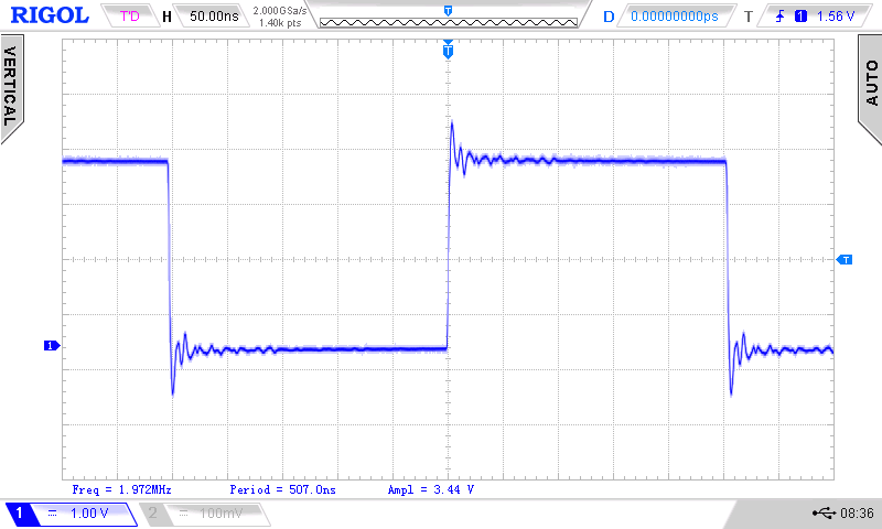
Click for a sharper view!
Yes it works but the frequency is weird. Ok we will fix this later.
If you have no oscilloscope, you can uncomment the two lines in mainloop and connect an LED with series resistor to the toggle pin. If you have a Pico2 (no W) you can use pin 25 for the onboard LED.
Let’s now look at the code:
Analysing the source code
The source code is a plain text file with the ending .asm (e.g. for RARS), or .s (no C preprocessor) .S (using C preprocessor).
The C preprocessor runs first and performs textual substitutions on the source code before passing it to the assembler. As we use the GCC assembler and I don’t know if I need the preprocessor in later examples, our files will have always big .S as ending.
There are no rules how to format the text file, but I will use 4 different columns and a tabulator with a tab size of 8 character.
-
Labels (1 column):
Mark addresses for jumps, data fields or strings. They should be explicit and end with a colon. Special labels begin with an underscore. -
Assembler directives (2 column):
Assembler directives start always with a dot (.). They are also called pseudo-opcodes and are instructions for the assembler (no executable instructions) that help with the assembly process. E.g. they define constants (.equ), reserve memory space for variables (.word), or set the program origin (.section .text). -
Op-codes (3 column):
Executable instructions in assembler. -
Comments (4 column):
The most important thing ;). They start with the number sign#(this can be confusing in combination with the C preprocessor (e.g. #define)). For comments over mor lines we can also use/* comment */like in C.
Directives, Sections, Data types and Definitions
There are 5 Section Directives: .text,.data, .rodata, .bss and .noinit.
In GCC we explicitly need to precede the needed directive with the directive .section.
-
.section.text: Beginning with this address in memory we find our program (assembler opcodes). -
.section.data: Address of data that needs to be written or read. -
.section.rodata: Read Only data
For the start of our program we find:
        .section .text                  # Marks the start of the code section in memory
        .global _start                  # Makes the symbol '_start' visible to the linker
The .global directive makes the special label (address) _start globally visible for the linker.
For data we can precise which data we use with Data types:
-
asciizor.ascii: Strings with quotation marks with or without NULL-Byte -
.byte,.hword,.word,.dword: 8, 16, 32, 64 bit -
.byte,.2byte,.4byte,.8byte: same as above but clearer -
.space: Reserves a number of bytes
Data types are often preceded by a label. The data itself is separated by commas.
For Definitions GCC uses .equ. GCC needs a comma after the symbol and can even do calculations:
        .equ PIN_OUT, 15
        .equ GPIO_MASK,       (1 << PIN_OUT)    # Bitmask for GPIO (e.g. GPIO15 = bit 15)
In this example it does a left shift of 15 bit, so the name GPIO_MASK is replaced with 0b00000000000000001000000000000000 = 0x0080.
The weird block
We want to use a RISC-V core. A block of 32 bytes (8 words) tells the chip what core to use. Here is the block with some comments:
        ### RP2350 Image Definition Block
        # This block is required for the RP2350 to recognize the binary as a valid
        # RISC-V executable. It must appear within the first 4 KB of the image.
        # RP2350 data sheet: 5.9.1. Blocks and block loops
        # 5.9.3. Image definition items, 5.9.3.4. ENTRY_POINT item
        .p2align 8       # Align to 8-byte boundary (required for RP2350 image header)
        .word 0xffffded3 # Header magic number (identifies the image)
        .word 0x11010142 # Item 0 flags: 0b0001 0001 0000 0001 0000 0100 0010
                         # IMAGE_TYPE_EXE, EXE_SECURITY_UNSPECIFIED,
                         # EXE_CPU_RISC,  EXE_CHIP_RP2350
        .word 0x00000344 # Item 1: Block size = 3,
                         # Block type = PICOBIN_BLOCK_ITEM_1BS_ENTRY_POINT
        .word _start     # Item 2: Inital PC (runtime) address (aka entry point)
        .word _stack_top # Item 3: Initial SP address (aka stack pointer)
        .word 0x000004ff # Item 4: Optional SP limit address (aka stack limit)
        .word 0x00000000 # Link: Single block loop has 0 items
        .word 0xab123579 # Footer magic number
In further programs we will use this block without comments.
Setting up a GPIO pin
To use a GPIO for digital I/O operations we need to configure some register. This is the price to pay for the flexibility of modern µC pins.
If we look at the RP2350 bus fabric overview (data sheet figure 5) we see that we have a high speed bus AHB5 and a low speed bus called APB. It gives access to system control registers and lower-bandwidth peripherals. But for our GPIO pins we have a separated single-cycle IO subsystem called SIO that is directly connected to the high speed bus.
The SIO peripherals are accessed via a dedicated path from each processor.
Multiplexing
Every pin can have different functions like SPIx, UARTx, I2Cx, SIO …. (1.2.3. GPIO functions (Bank 0), 9.4. Function select). We need here the SIO function (function nr 5) that handles all user GPIOs (3.1.3. GPIO control).
GPIO functions are on User Bank 0. The User Bank IO registers start at a base address of 0x40028000 defined as IO_BANK0_BASE (9.11.1. IO - User Bank). To multiplex our output pin to the GPIO function we need the GPIO_CTRL register at address 0x4002807C. It is no good idea to use absolute addresses, so we need an offset of 0x07C to the base address. To make our program flexible we let the assembler calculate the offset!
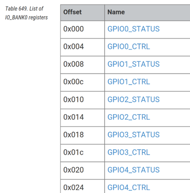
Figure 1. List of IO_BANK_0 register (RP2350 data sheet)
We see that the offset increments by four for each register. We have a Status- and a Ctrl-Register per GPIO pin, so the formula for the offset is: GPIO_OFFSET = pin_number*8+4, e,g. 15*8+4 = 124 = 0x7C.
        .equ PIN_OUT, 15
        .equ GPIO_OFFSET,     PIN_OUT*8+4   # Offset for GPIO reg. (0=Status, +4=Ctrl)
        .equ IO_BANK0_BASE,   0x40028000        # IO Bank0 Base Address
        .equ GPIO_CTRL,       IO_BANK0_BASE + GPIO_OFFSET # GPIO_CTRL reg. (for Mux)

                # SETUP: Tell the multiplexer to set our Pin to GPIO
                li t0, GPIO_CTRL    # Load the address of the GPIO_CTRL reg. to t0
                lw t1, 0(t0)        # Load current value of the GPIO_CTRL reg. to t1
                andi t1, t1, ~0x1F  # Clear the lower 5 bits (function select)
                ori t1, t1, 5       # Set the function select to 5 (GPIO mode)
sw t1, 0(t0) # Store updated value back to the GPIO_CTRL reg.TASK:
We need to write 0x0005 (function 5: select GPIO (SIO) for the pin) to the GPIO_CTRL register corresponding to our pin (e.g. GPIO15_CTRL). We do it by masking with AND to clear bits and OR to set bits. So other bits in the register than the lower 5 bits are not changed.
FUNCSEL: 0-31 → selects pin function according to the gpio table
| instruction | op code | source | destination |
|---|---|---|---|
|
|
address |
temporary register |
|
|
content of |
temporary register |
|
|
content t1 |
temporary register |
|
|
content of the |
temporary register |
|
|
temporary register |
|
Remarks:
-
The instructions wit
iuse immediate addressing meaning the number used is in the instruction. -
The two other instructions (load and store word) use indirect addressing! The instruction gets the register with the address in parentheses. The zero is an offset that can be added to the address, but as we need no offset it is 0.
-
We could have used atomic commands to manipulate the bits, but this would make the code here bigger.
-
The
~inverts the number 0x1F to 0xFE0 (12 bit). This is done by GCC before assembling. -
As
andican handle signed immediate numbers up to 12 bit, but as we need here a mask with 32 bit this could be a problem. Butandiis a pseudo instruction, so the assembler is able to sign-extended the 12-bit immediate correctly to 32 bits (here 0xFFFFFFE0) before the real operation (withluiandauipc).
Set direction of GPIO
Next we need to set the GPIO to output. For this we use the
        .equ GPIO_MASK,       (1 << PIN_OUT)    # Bitmask for GPIO (GPIO15 = bit 15)
        .equ GPIO_DIR,        SIO_BASE + 0x30   # GPIO direction register

### SETUP: Set GPIO15 as an output
                li t0, GPIO_DIR     # Load the address of the GPIO direction register
                lw t1, 0(t0)        # Load current value of the direction reg. to t1
                li t2, GPIO_MASK    # Load the bitmask for the used GPIO
                or t1, t1, t2       # Set the bit for used GPIO (output mode)
                sw t1, 0(t0)        # Store updated value back to the GPIO dir. reg.
.equ ATOMIC_XOR, 0x1000 # atomic XOR on write
.equ ATOMIC_SET, 0x2000 # atomic bitmask set on write
.equ ATOMIC_CLR, 0x3000 # atomic bitmask clear on write
.equ GPIO_MASK, (1 << PIN_OUT) # Bitmask for GPIO (GPIO15 = bit 15)
.equ GPIO_DIR, SIO_BASE + 0x30 # GPIO direction register
.equ GPIO_DIR_SET, SIO_BASE + 0x30 + ATOMIC_SET # GPIO dir to output
.equ GPIO_DIR_CLR, SIO_BASE + 0x30 + ATOMIC_SET # GPIO dir to input
### SETUP: Set GPIO15 as an output
li t0, GPIO_DIR # Load the address of the GPIO direction register
lw t1, 0(t0) # Load current value of the direction reg. to t1
li t2, GPIO_MASK # Load the bitmask for the used GPIO
or t1, t1, t2 # Set the bit for used GPIO (output mode)
sw t1, 0(t0) # Store updated value back to the GPIO dir. reg.Pad isolation
Look at the drive strength parameter (2 bit) default = 0b01 = 4mA (0b11 = 12mA) DRIVE: Drive strength.
        .equ PIN_OUT, 15
        .equ GPIO_OFFSET,     PIN_OUT*8+4   # Offset for GPIO reg. (0=Status, +4=Ctrl)
        .equ IO_BANK0_BASE,   0x40028000        # IO Bank0 Base Address
        .equ GPIO_CTRL,       IO_BANK0_BASE + GPIO_OFFSET # GPIO_CTRL reg. (for Mux)


                # SETUP: Tell the multiplexer to set our Pin to GPIO
                li t0, GPIO_CTRL    # Load the address of the GPIO_CTRL reg. to t0
                lw t1, 0(t0)        # Load current value of the GPIO_CTRL reg. to t1
                andi t1, t1, ~0x1F  # Clear the lower 5 bits (function select)
                ori t1, t1, 5       # Set the function select to 5 (GPIO mode)
                sw t1, 0(t0)        # Store updated value back to the GPIO_CTRL reg.
Debugging with DebugProbe, OpenOCD and GDB
With Debug Probe, you can load binaries via the SWD port and OpenOCD. First, build a binary. Then, run the following command to upload the binary to the Pico, replacing blink.elf with the name of the ELF file you just built:
openocd -f interface/cmsis-dap.cfg -f target/rp2350.cfg -c "adapter speed 5000" -c "program blink.elf verify reset exit"
For this we need two terminal windows. In the first window we use openocd to open a TCP/IP port to communicate with gdb:
cd
openocd -f interface/cmsis-dap.cfg -f target/rp2350-riscv.cfg -c "adapter speed 5000"
The last lines of the should be
...
Info : [rp2350.rv1] Examined RISC-V core
Info : [rp2350.rv1]  XLEN=32, misa=0x40901105
Info : [rp2350.rv1] Examination succeed
Info : [rp2350.rv0] starting gdb server on 3333
Info : Listening on port 3333 for gdb connections
We add the -g flag to our gcc command to get debug info added to our elf. file
(Before running gdbgui, you should compile your program with debug symbols and a lower level of optimization, so code isn’t optimized out before runtime. To include debug symbols with gcc use -ggdb, with rustc use -g. To disable most optimizations in gcc use the -O0 flag, with rustc use -O.)
file 02_toggle_tidy.elf 02_toggle_tidy.elf: ELF 32-bit LSB executable, UCB RISC-V, RVC, soft-float ABI, version 1 (SYSV), statically linked, not stripped file 02_toggle_tidy.elf 02_toggle_tidy.elf: ELF 32-bit LSB executable, UCB RISC-V, RVC, soft-float ABI, version 1 (SYSV), statically linked, with debug_info, not stripped
In a second terminal we start gdb with the name of our .elf file:
cd
riscv32-corev-elf-gdb 02_toggle_tidy.elf
Here the last 2 lines after the command and the (gdb) prompt. Now we can enter commands in gdb.
...
Reading symbols from 02_toggle_tidy.elf...
(No debugging symbols found in 02_toggle_tidy.elf)
(gdb)
The first command target extended-remote :3333 tells gdb where to listen
target extended-remote :3333 monitor reset init
break main run
next (n) does not enter subroutines step () does enter subroutines list lists 10 lines
info registers (i r)
continue (c)
An C? print (p) to look at a var, can also calculate
display /x $t0 display /t $t1
Here a small debug session going stepwise (command n) through our first program lines (I reformatted the output a little to get a better grip of things):
                           $t0 = 0x0         $t1 = 110101000101100
38 li t0, GPIO_CTRL
                           $t0 = 0x4002807c  $t1 = 110101000101100
39 lw t1, 0(t0)
                           $t0 = 0x4002807c  $t1 = 11111           # default after reset!
40 andi t1, t1, ~0x1F
                           $t0 = 0x4002807c  $t1 = 0               # clear 5 bit
41 ori t1, t1, 5
                           $t0 = 0x4002807c  $t1 = 101             # set 2 bit
42 sw t1, 0(t0)
                           $t0 = 0x4002807c  $t1 = 101
45 li t0, GPIO_DIR_SET
                           $t0 = 0xd0002030  $t1 = 101              # atomic
46 li t1, GPIO_MASK
                           $t0 = 0xd0002030  $t1 = 1000000000000000 # bit 15
47 sw t1, 0(t0)
                           $t0 = 0xd0002030  $t1 = 1000000000000000
9.11.3. Pad Control - User Bank
9.6. Pads
Each GPIO is connected off-chip via a pad. Pads are the electrical interface between the chip’s internal logic and external circuitry. They translate signal voltage levels, support higher currents and offer some protection against electrostatic discharge (ESD) events. You can adjust pad electrical behaviour to meet the requirements of external circuitry in the following ways: • Output drive strength can be set to 2mA, 4mA, 8mA or 12mA. • Output slew rate can be set to slow or fast. • Input hysteresis (Schmitt trigger mode) can be enabled. • A pull-up or pull-down can be enabled, to set the output signal level when the output driver is disabled. • The input buffer can be disabled, to reduce current consumption when the pad is unused, unconnected or connected to an analogue signal. An e
RP2350 has isolation latches on all GPIO (RP2040 only on some). We need to enable the pad input (GPIO0.IE = 1) and disable pad isolation latches (GPIO0.ISO = 0) before using the pads for digital I/O. If the SDK is used this is done with the function gpio_set_function().
Pad isolation is needed for extended low-power states. More info in chapter 9.7. (Pad isolation latches) in the RP2350 data sheet.
equ PAD_ISO_REG, 0x40038000 + 0x40 # Pad isolation control register for GPIO15
 1
 2
 3
 4
 5
 6
 7
 8
 9
10
11
12
13
14
15
16
17
18
19
20
21
22
23
24
25
26
27
28
29
30
31
32
33
34
35
36
37
38
39
40
41
42
43
44
45
46
47
48
49
50
51
52
53
54
55
56
57
58
59
60
61
62
63
### Toggle an GPIO pin (minimal tidy version)
### 01_toggle_tidy.S
### we use more files and include them to get a tidy version :)
### weigu.lu

# Required for the RP2350 to recognize the binary as a valid RISC-V executable.
#include "rp2350_riscv_image_def_block.S"
#include "sr_delays.S"

//#define LED_ONBOARD

        ### Global vars
        #ifdef LED_ONBOARD
        .equ PIN_OUT, 25            # Pin to use, needed for the register def.
        #else
        .equ PIN_OUT, 15            # Pin to use, needed for the register def.
        #endif
        .equ DELAY_NUMBER, 1000000  # 1000000 gives us ~ 2 Hz (12MHz clock)

# Must come after ".equ PIN_OUT" because this value is needed to calculate register
#include "rp2350_reg_definitions.S"

        .section .text              # Marks the start of the code section in memory
        .global _start              # Makes the symbol '_start' visible to the linker

### Entry Point: _start
_start:         la sp, _stack_top   # Load the stack pointer with the top of the stack
                call main           # Call the main function
                wfi                 # Wait for interrupt (low-power mode)
                j _start            # Infinite loop (should never reach here)

### Main Function
        .section .text              # Code section
        .global main                # Make 'main' visible to the linker

main:
                # SETUP: Tell the multiplexer to set our Pin to GPIO
                li t0, GPIO_CTRL    # Load the address of the GPIO_CTRL reg. to t0
                lw t1, 0(t0)        # Load current value of the GPIO_CTRL reg. to t1
                andi t1, t1, ~0x1F  # Clear the lower 5 bits (function select)
                ori t1, t1, 5       # Set the function select to 5 (GPIO mode)
                sw t1, 0(t0)        # Store updated value back to the GPIO_CTRL reg.

                ### SETUP: Set GPIO15 as an output
                li t0, GPIO_DIR_SET  # Load the address of the GPIO direction register
                li t1, GPIO_MASK    # Load the bitmask for the used GPIO
                sw t1, 0(t0)        # Store updated value back to the GPIO dir. reg.

                ### Setup: Clear Pad Isolation for GPIO
                li t0, PAD_CLR       # Load the address of the pad register
                li t1, PAD_MASK_ISO_BIT # Load the bitmask for the used GPIO
                sw t1, 0(t0)         # Store updated value back to the register

                li t0, GPIO_OUT_XOR # Load the address of the GPIO_OUT_XOR
                li t1, GPIO_MASK    # Load the bit for the output GPIO to be toggled

mainloop:       # Main Loop: Toggle output on GPIOx
                sw t1, 0(t0)        # Set the bit (atomic bit setting-writing)
                #ifdef LED_ONBOARD
                li a0, DELAY_NUMBER # set counter for delay loop (parameter a0)
                jal simple_delay_a0           # jump and link delay (command call bor big jumps)
                #endif
                j mainloop          # jump mainloop forever
How to reset the pico2 if everything goes wrong
If you are no more able to program the pico or if the clock speed is false we need to reset the chip in its original state. To do so need to power it with pressed bootsel button. This will cause the Pico to appear as a removable drive, where we erase all files on this drive to reset it completely.
Downloads
-
Everything on github: [https://github.com/weigu1/rpi_pico_pio](https://github.com/weigu1/rpi_pico_pio)
Interesting links
http://blog.wolfman.com/articles/2025/5/19/bare-metal-gpio-twiddling-for-risc-v-on-rpi-pico2 https://github.com/wolfmanjm/RISC-V-RP2350-baremetal https://mcyoung.xyz/2021/11/29/assembly-1/ https://smist08.wordpress.com/2024/10/21/risc-v-on-the-raspberry-pi-pico-2/
+ SDK on github: https://github.com/raspberrypi/pico-sdk + SDK: https://datasheets.raspberrypi.com/pico/raspberry-pi-pico-c-sdk.pdf + Datasheet RP2350: https://datasheets.raspberrypi.com/rp2350/rp2350-datasheet.pdf + Getting started with Pico (pdf): https://datasheets.raspberrypi.com/pico/getting-started-with-pico.pdf + Picotool: https://github.com/raspberrypi/picotool
<br> <br>
