Microcontroller projects
GHIDRA: Bare-metal ARM reverse engineering
last updated: 2021-03-06
Introduction
Ghidra is a free and open source reverse engineering tool, developed by the National Security Agency (NSA). The sources (java and C++) were published in 2019 on GitHub.

We will use Ghidra to reverse engineer microcontroller code from an STM32 microcontroller. This is called "bare-metal" because the µC has no operating system and no driver. The application runs directly on the hardware.
A really cool video about this topic can be found here: https://youtu.be/q4CxE5P6RUE.
Reverse engineering simple blink program on an STM32L152RE
Under STM32 I describe how to program the STM32L152RE chip using STM32CubeIDE and a NUCLEO-board.
Now we have a binary file and a list file that will help do reverse engineer the code (under Downloads at the end of the page).
Configuring Ghidra
After installing Ghidra we create a new non-shared project. Then we drop the binary file we want to analyse into the active project window (or File -> Import file).
We click on our file to start the codebrowser (dragon).
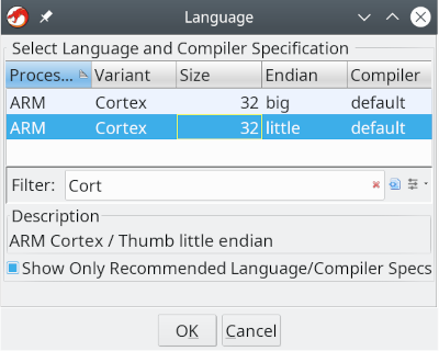
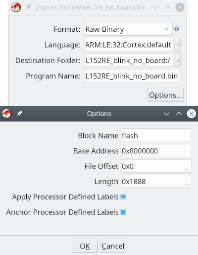
In the import window we need to precise the language. In the filter field we type "Cortex" and choose the version with little Endian. Under Options we define the flash (base) address witch is 0x8000000 for the STM32 chips and name it flash.


Before analysing the file (click "no") we will configure the memory map by opening the memory map window.

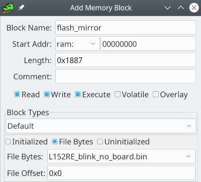
As explained on the STM32 page our Flash is mirrored. The normal boot starts at 0x00000000. So we create a new memory block called "flash_mirror" with address 0x0000000 and mark it as executable. We give the block the same length than the file (0x1888) and an File Offset of 0x0 (mark "File Bytes"). Then we also define the RAM. In the data sheet we see that it is located at 0x20000000 and has a length of 80kByte.


Our memory map is not complete, because all the peripherals (GPIO etc) are mapped in memory. Fortunately we get help with SVD files, and a loader written by "leveldown-security".
SVD files contain a peripheral description of a device. The CMSIS-SVD format is based on XML and is a description of the device.
The loader is a python script that can be found on https://github.com/leveldown-security/SVD-Loader-Ghidra.
First we open the "Script Manager" (green disk with white arrow) and look for the icon called "Manage Script Directories" (list). Here we add the directory to the downloaded (and extracted) files with the loader script. After this we find a folder named "leveldown-security" in our list. By clicking on the script we can add the SVG file.
But where do we get the right file? A good starting point is the following link:
https://github.com/posborne/cmsis-svd/. Unfortunately the file I needed was corrupt. So I also locked here: https://www.keil.com/dd2/pack/#/eula-container and found a pack file for the STML152 chips. To get the SVD files we need to rename the KEIL .pack file to .zip and extract the SVD files.
After loading the SVD file we are ready to analyse the file (Analysis -> Auto analyse). Here we enable the "ARM Aggressive Instruction Finder" to get better results.
Find the RESET vector
Finally we can look at the code. In the Menu we get the Window. it's a good starting point to look and test the different Windows. It is frightening because the Function window shows 67 functions for such a little program. So the overhead is huge and not what we are used when programming AVR cores!
The RESET interrupt vector is located at address 0x00000004. So here we get the address of some main function (0x660).

In this function we do not find our program, but two loops and 3 calls. Fortunately we have our list file and can see that at 0x660 there is a comment:
/* Copy the data segment initializers from flash to SRAM */0x67a:
/* Zero fill the bss segment. */That's for the loops. The first function at 0x648 is a SystemInit function and the second function at 0x17e0 is marked with __libc_init_array.
    void UndefinedFunction_0000065c(undefined4 param_1) {
      int iVar1;
      undefined4 *puVar2;
      undefined4 in_cr14;
      coprocessor_store(0,in_cr14,param_1);
      iVar1 = 0;
      while (puVar2 = (undefined4 *)PTR_DAT_000006a0, PTR_DAT_00000698 + iVar1 < PTR_DAT_0000069c) {
        *(undefined4 *)(PTR_DAT_00000698 + iVar1) = *(undefined4 *)(PTR_DAT_00000694 + iVar1);
        iVar1 = iVar1 + 4;
      }
      while (puVar2 < PTR_DAT_000006a4) {
        *puVar2 = 0;
        puVar2 = puVar2 + 1;
      }
      FUN_00000648();
      FUN_000017e0();
      FUN_00000480();
      return;
    }
But for the third function (0x480) we recognise our program:
Main program
    void FUN_00000480(void) {
      FUN_000006aa();
      FUN_000004a4();
      FUN_00000534();
      do {
        FUN_00000ce0(PTR_GPIOA_000004a0,0x20);
        FUN_00000788(200);
      } while( true );
    }
    #include "main.h"
    void SystemClock_Config(void);
    static void MX_GPIO_Init(void);
    int main(void) {
      HAL_Init();
      SystemClock_Config();
      MX_GPIO_Init();
      while (1) {
        HAL_GPIO_TogglePin(GPIOA,LED);
        HAL_Delay(200);
      }
    }
HAL_init() at 0x6aa, SystemClock_Config() at 0x4a4 and MX_GPIO_Init() at 0x534.
MX_GPIO_Init()
Let's first look at the MX_GPIO_Init() function:
    static void MX_GPIO_Init(void) {
      GPIO_InitTypeDef GPIO_InitStruct = {0};
      __HAL_RCC_GPIOA_CLK_ENABLE();    /* GPIO Ports Clock Enable */
      HAL_GPIO_WritePin(GPIOA, GPIO_PIN_5, GPIO_PIN_RESET); /*Configure GPIO pin Output Level */
      GPIO_InitStruct.Pin = GPIO_PIN_5; /*Configure GPIO pin : PA5 */
      GPIO_InitStruct.Mode = GPIO_MODE_OUTPUT_PP;
      GPIO_InitStruct.Pull = GPIO_NOPULL;
      GPIO_InitStruct.Speed = GPIO_SPEED_FREQ_LOW;
      HAL_GPIO_Init(GPIOA, &GPIO_InitStruct);
    }
In Ghidra we find (comments added by comparison):
void FUN_00000534(void) {
  undefined4 local_1c; // GPIO_InitTypeDef GPIO_InitStruct = {0};
  undefined4 local_18;
  undefined4 local_14;
  undefined4 local_10;
  undefined4 local_c;
  local_1c = 0;
  local_18 = 0;
  local_14 = 0;
  local_10 = 0;
  local_c = 0;
  //__HAL_RCC_GPIOA_CLK_ENABLE()
  *(uint *)(PTR_RCC_0000058c + 0x1c) = *(uint *)(PTR_RCC_0000058c + 0x1c) | 1;
  // HAL_GPIO_WritePin(GPIOA, GPIO_PIN_5, GPIO_PIN_RESET);
  FUN_00000cb0(PTR_GPIOA_00000590,0x20,0,*(uint *)(PTR_RCC_0000058c + 0x1c) & 1);
  local_1c = 0x20;  // GPIO_InitStruct.Pin = GPIO_PIN_5;
  local_18 = 1;     // GPIO_InitStruct.Mode = GPIO_MODE_OUTPUT_PP;
  local_14 = 0;     // GPIO_InitStruct.Pull = GPIO_NOPULL;
  local_10 = 0;     //GPIO_InitStruct.Speed = GPIO_SPEED_FREQ_LOW;
  FUN_00000994(PTR_GPIOA_00000590,&local_1c); // HAL_GPIO_Init(GPIOA, &GPIO_InitStruct);
  return;
}
Ok to understand this we must look deeper in the GPIO register. After a RESET the ports are configured as analogue input. Each Port has 4 configuration register (GPIOx_MODER, GPIOx_OTYPER, GPIOx_OSPEEDR and GPIOx_PUPDR), 2 data register (GPIOx_IDR, GPIOx_ODR), 1 bit set/reset register (GPIOx_BSRR), 1 bit locking register (GPIOx_LCKR) and 2 alternate function register (GPIOx_AFRH, GPIOx_AFRL). All register are 32 bit register and they can be accessed with one, two or 4 bytes.
We find the addresses in Ghidra and they correspond to our memory map (STM32):
- PTR_RCC_0000058c =
0x40023800// 0x58c: addressRCC(Reset + Clock Control) = 0x40023800 - PTR_GPIOA_00000590 =
0x40020000// 0x590: address PeripheralsGPIOA= 0x40020000
By looking in the Reference manual RM0038 (st.com) we also find the offsets:
0x40023800 + 0x1c is the RCC_AHBENR register. With setting the first bit to 1 (or mask) we enable GPIOA clock.
Pin number 5 is coded in 0x20 = 0b00100000, because pin 5 is set.
FUN_00000994() is huge and sets all the different bits in the GPIO register using the structure.
HAL_GPIO_TogglePin()
HAL_GPIO_TogglePin(GPIOA,LED) gives the following code in Ghidra:
FUN00000ce0(PTRGPIOA_000004a0,0x20);
Let's look at the first parameter:
- PTR_GPIOA_000004a0 =
0x40020000// 0x4a0: address PeripheralsGPIOA= 0x40020000
Here we get the same GPIOA base address as on memory location 0x590. The second parameter 0x20 is Pin 5.
    void FUN_00000ce0(int param_1,ushort param_2) {
      *(uint *)(param_1 + 0x18) =
           (*(uint *)(param_1 + 0x14) & (uint)param_2) << 0x10 |
           (uint)param_2 & ~*(uint *)(param_1 + 0x14);
      return;
}
Param1 + 0x18 is the bit set/reset register BSSR. Param1 + 0x14 is the input data register IDR, so we read the bit. We get BSSR = IDR & (0x20<<0x10) | 0x20 & (~IDR).
The bit is toggled using a classical XOR function!
Yes it is possible to completely reverse engineer code, but it is very time consuming, especially when the code is bloated like the STM32 code created with the STM32CubeIDE.
Closing claim
Yes it is possible to completely reverse engineer code, but it is very time consuming, especially when the code is bloated like the STM32 code created with the STM32CubeIDE.
Downloads
Interesting links:
- https://github.com/leveldown-security/SVD-Loader-Ghidra
- https://github.com/posborne/cmsis-svd/.
- https://www.keil.com/dd2/pack/#/eula-container
- https://github.com/dmitrystu/svd_editor
