Microcontroller projects
STM32
last updated: 2021-03-06
Introduction
While investigating some IoT devices, I found that quite often microcontroller from STMicroelectronics (st.com) are used, especially the STM32 ARM Cortex (M0, M3, M4) processors. Here I will document my first trials with these µC.
- Important:
There are many many different STM32 µC. The last characters of the chips naming (e.g. STM32L152RE) are here most important, because pin number, housing and size of the memory change with this characters.
Closing claim
I will not use these chips for my own projects.
- The main problem is that I didn't find easily cool libraries to help while programming. Rewriting all functions for Serial, Software I2C, integrated LCD and LoRa chips it is too time consuming.
- The Arduino core didn't support the chips I wanted to use, so no relief here.
- It is cool that the
STM32CubeIDEruns under Linux, but I did not like the HAL layer producing 1888 bytes of code for a simple blink program. Here you can read how I reverse engineered the code withghidra. Also cloning projects was not straightforward, and I got sometimes strange errors (java nullpointer?). And example projects with libraries could be integrated in the IDE (If they are there, I did not find them.
So I will continue to use Teensy boards with Cortex microcontroller. Paul wrote so cool Arduino libs. And I look forward what the new RISC-V will bring.
Programming
Programmer ST-LINK/V2
To program the STM32 we need a ST-LINK/V2 programmer. A JTAG/serial wire debugging (SWD) interface is used to communicate with the chip.
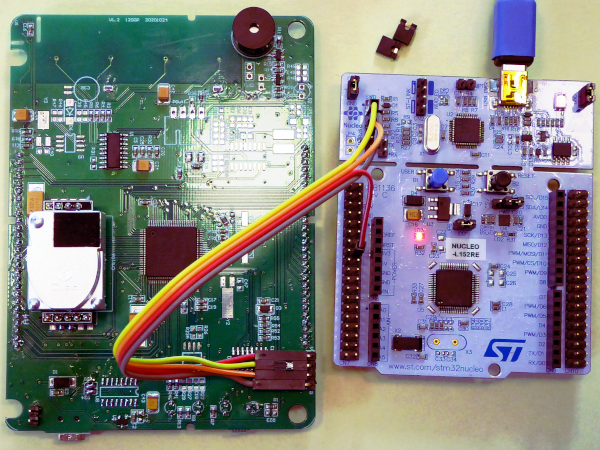
The easiest way to get one is to buy a NUCLEO board. These prototyping boards include a programmer that can be used to program external chips.

From the 6 pin SWD header we need pins only 3 pins:
| PIN Nr | SIGNAL | |
|---|---|---|
| 2 | SWCLK | SWD clock |
| 3 | GND | Ground |
| 4 | SWDIO | SWD data (input/output) |
Software
The NUCLEO boards can be easily programmed with Mbed OS online.
But there are also two new interesting and free software packages from STM. The STM32CubeIDE and the STM32CubeProgrammer. Both are running under Linux, so worth to giving a try.
Blink with the STM32CubeIDE
To run a first program I use a NUCLEO-L152RE. The STM32L152RE in LQFP64 package contains an ARM®32-bit Cortex®-M3 CPU using the Armv7-M instruction set (ISA).
After installing the STM32CubeIDE we create a workspace and choose a workspace folder. Then create a new STM32 Project. Now we can choose a µC or a board. We choose the µC STM32L152RE and not the NUCLEO board to get a shorter program code, because later we want to analyse it with Ghidra.
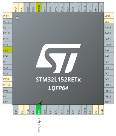
We give the project a name and the project is created presenting us the pinout of the chip in an .ioc-file:

We click on PA5 and define the pin as an output (the green LED on the Nucleo board is connected to this pin). This spares us from writing the code, because the code is automatically generated. The same applies if we want to change the clock settings. This can be done in the "Clock Configuration" tab. After the changes we must save the file (File -> save) to get the code generated.
In the Project Explorer we go to Core -> Src and choose the main file (main.c). If we omit the comments we get the following code:
    #include "main.h"
    void SystemClock_Config(void);
    static void MX_GPIO_Init(void);
    int main(void) {
      HAL_Init();
      SystemClock_Config();
      MX_GPIO_Init();
      while (1) {
        // here comes my code
      }
    }
We see that after the declarations 3 init functions are called, and then comes the main loop (while (1) {}). HAL_Init() initialises the Hardware Abstraction Layer. Both other functions were generated automatically and the code can be see under the main function. Let's take a short look at the initialisation of the GPIO.
    static void MX_GPIO_Init(void) {
      GPIO_InitTypeDef GPIO_InitStruct = {0};

      /* GPIO Ports Clock Enable */
      __HAL_RCC_GPIOA_CLK_ENABLE();

      /*Configure GPIO pin Output Level */
      HAL_GPIO_WritePin(GPIOA, GPIO_PIN_5, GPIO_PIN_RESET);

      /*Configure GPIO pin : PA5 */
      GPIO_InitStruct.Pin = GPIO_PIN_5;
      GPIO_InitStruct.Mode = GPIO_MODE_OUTPUT_PP;
      GPIO_InitStruct.Pull = GPIO_NOPULL;
      GPIO_InitStruct.Speed = GPIO_SPEED_FREQ_LOW;
      HAL_GPIO_Init(GPIOA, &GPIO_InitStruct);
    }
We see that the pin is 5 of port A is defined as output with enabled clock, no pull up resistor and a low frequency. Everything is saved in a structure.
Let's now toggle the LED. Here is the code for the main loop:
    #define LED GPIO_PIN_5
    while (1) {
        HAL_GPIO_TogglePin(GPIOA,LED);
        HAL_Delay(200);
    }
Finally we can click on the "Run Debug" icon to compile and program the chip. The LED is blinking.
in the DEBUG folder of the project we find the binary or hex-file (.bin) that is programmed to the Flash memory at address 0x800000 and the list file, that shows all the assembler code. These files are interesting when we try to reverse engineer the code with ghidra.
Memory map and boot
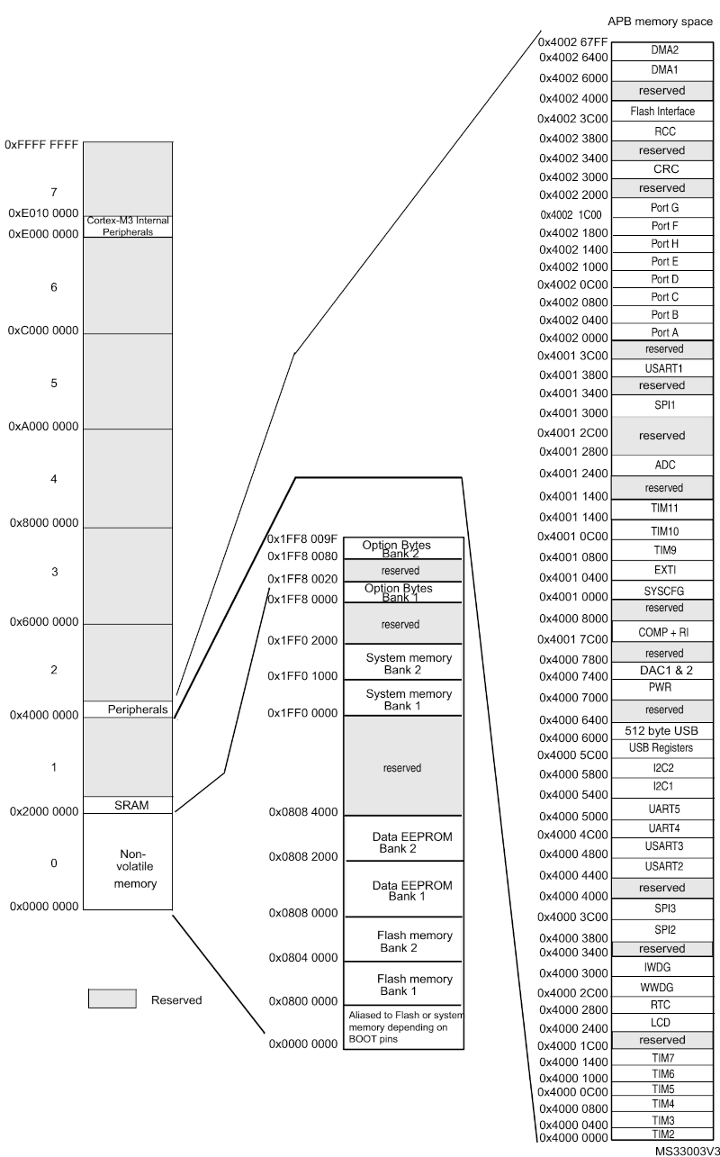
If we look at our data sheet we see that our chip (L152RE) has 512 kbytes of Flash memory, 80 kbytes of RAM, 16 kbytes of true EEPROM and an 128-byte backup register. In the data sheet we find the following picture:

Nonvolatile memory (Flash EEPROM) beginns at 0x00000000, RAM at 0x20000000 and the Peripherals at 0x40000000.
The Flash (memory bank 1) begins at 0x0800000 (bank 1 = 256kbyte, bank 2 = 256kbyte) but it is mirrored to 0x00000000, if the boot pins are set accordingly. So what are these boot pins?
Under "Boot modes" we find an explanation in the data sheet:
At startup, boot pins are used to select one of three boot options:
+ Boot from Flash memory (normally bank 1, through user option byte bank 2 can be chosen).
+ Boot from System memory. A bootloader is located in System memory. It gives the possibility to reprogram the Flash memory by using USART1, USART2 or USB (DFU bootloader) (look for Application note AN2606).
+ Boot from embedded RAM
So we have two Boot pins. Boot pin 0 (green) can be easily found between PB7 and PB9 in our pinout view (see above). In normal mode it is LOW (data sheet NUCLEO Board: The default state of BOOT0 is LOW), an we boot from Flash if there is valid data on bank 1 or 2. Boot pin 2 is PB2 and it is only needed if we want to use the bootloader.
Serial with the STM32CubeIDE
Choose the pins with the hardware USART (e.g. PB6 USART1-TX, PB7 USART1-RX) and config them in the Pinout View. Then click on Connectivity and choose your USART. Now choose in Mode "Asynchronous" and select your data frame and the bit-rate in Configuration.
For the clock choose HSI-16.
We add the following code. Pay attention to place your code where the comments suggest, otherwise it will be overridden when code is generated by the device configuration tool.
    /* USER CODE BEGIN Includes */
    #include "string.h"
    ...
    /* USER CODE BEGIN PFP */
    void serial1_send(char buffer[]) {
        if (HAL_UART_Transmit(&huart1, (uint8_t*) buffer, strlen(buffer), HAL_MAX_DELAY) != HAL_OK) {
            Error_Handler();
        }
    }
    ...
    /* USER CODE BEGIN WHILE */
    while (1)  {
        serial1_send("Hello Serial\n");
        HAL_Delay(100);
    }
Downloads
Interesting links:
- Reverse engineering STM32 code with
ghidra: http://weigu.lu/microcontroller/ghidra_nsa/index.html
